- 您现在的位置:买卖IC网 > Sheet目录334 > ISL8510EVAL1Z (Intersil)EVALUATION BOARD FOR ISL8510
�� �
�
�ISL8510�
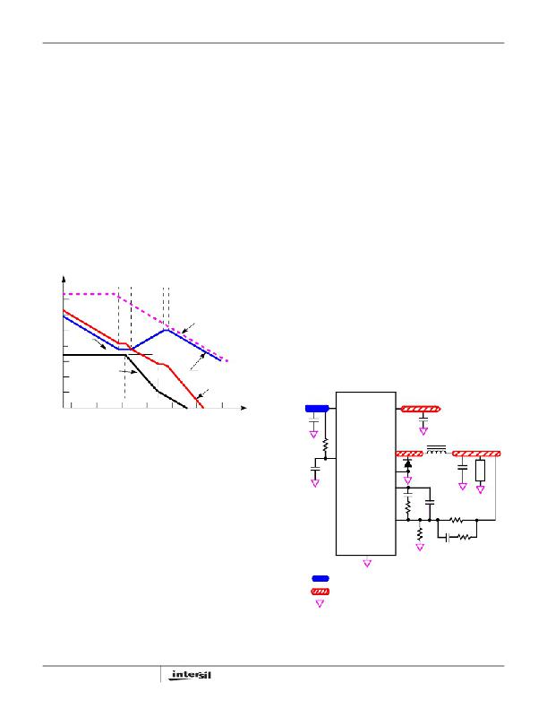
�Figure� 31� shows� an� asymptotic� plot� of� the� DC/DC�
�converter� ’s� gain� vs� frequency.� The� actual� Modulator� Gain�
�has� a� high� gain� peak� due� to� the� high� Q� factor� of� the� output�
�filter� and� is� not� shown� in� Figure� 31.� Using� the� guidelines�
�from� “Modulator� Break� Frequency� Equations”� on� page� 18�
�should� give� a� Compensation� Gain� similar� to� the� curve�
�plotted.� The� open� loop� error� amplifier� gain� bounds� the�
�compensation� gain.� Check� the� compensation� gain� at� f� P2�
�with� the� capabilities� of� the� error� amplifier.� The� Closed� Loop�
�Gain� is� constructed� on� the� graph� of� Figure� 31� by� adding� the�
�Modulator� Gain� (in� dB)� to� the� Compensation� Gain� (in� dB).�
�This� is� equivalent� to� multiplying� the� modulator� transfer�
�function� to� the� compensation� transfer� function� and� plotting�
�the� gain.�
�The� compensation� gain� uses� external� impedance� networks�
�Z� FB� and� Z� IN� to� provide� a� stable,� high� bandwidth� (BW)� overall�
�loop.� A� stable� control� loop� has� a� gain� crossing� with�
�-20dB/decade� slope� and� a� phase� margin� greater� than� 45°.�
�Include� worst� case� component� variations� when� determining�
�phase� margin.�
�load� current.� During� turn-off,� current� stops� flowing� in� the�
�MOSFET� and� is� picked� up� by� the� lower� MOSFET.� Any�
�parasitic� inductance� in� the� switched� current� path� generates� a�
�large� voltage� spike� during� the� switching� interval.� Careful�
�component� selection,� tight� layout� of� the� critical� components,�
�and� short,� wide� traces� minimizes� the� magnitude� of� voltage�
�spikes.�
�There� are� two� sets� of� critical� components� in� the� ISL8510�
�switching� converter.� The� switching� components� are� the� most�
�critical� because� they� switch� large� amounts� of� energy,� and�
�therefore� tend� to� generate� large� amounts� of� noise.� Next� are�
�the� small� signal� components,� which� connect� to� sensitive�
�nodes� or� supply� critical� bypass� current� and� signal� coupling.�
�A� multi-layer� printed� circuit� board� is� recommended.�
�Figure� 32� shows� the� connections� of� the� critical� components�
�in� the� converter.� Note� that� capacitors� C� IN� and� C� OUT� could�
�each� represent� numerous� physical� capacitors.� Dedicate� one�
�solid� layer� (usually� a� middle� layer� of� the� PC� board)� for� a�
�ground� plane� and� make� all� critical� component� ground�
�connections� with� vias� to� this� layer.� Dedicate� another� solid�
�100�
�f� Z1� f� Z2�
�f� P1�
�f� P2�
�layer� as� a� power� plane� and� break� this� plane� into� smaller�
�islands� of� common� voltage� levels.� Keep� the� metal� runs� from�
�80�
�the� PHASE� terminals� to� the� output� inductor� short.� The� power�
�60�
�40�
�20LOG�
�OPEN� LOOP�
�ERROR� AMP� GAIN�
�plane� should� support� the� input� power� and� output� power�
�nodes.� Use� copper� filled� polygons� on� the� top� and� bottom�
�circuit� layers� for� the� phase� nodes.� Use� the� remaining� printed�
�20�
�(R� 2� /R� 1� )�
�20LOG�
�circuit� layers� for� small� signal� wiring.� The� wiring� traces� from�
�0�
�-20�
�MODULATOR�
�GAIN�
�(V� IN� /� Δ� V� OSC� )�
�COMPENSATION�
�GAIN�
�the� GATE� pins� to� the� MOSFET� gates� should� be� kept� short�
�and� wide� enough� to� easily� handle� the� 1A� of� drive� current.�
�-40�
�-60�
�10�
�100�
�1k�
�f� LC�
�10k�
�f� ESR�
�100k�
�1M�
�CLOSED� LOOP�
�GAIN�
�10M�
�5V�
�PVCC�
�VIN�
�V� IN�
�FREQUENCY� (Hz)�
�C� BP1�
�ISL8510�
�C� IN�
�FIGURE� 31.� ASYMPTOTIC� BODE� PLOT� OF� CONVERTER� GAIN�
�A� more� detailed� explanation� of� voltage� mode� control� of� a�
�buck� regulator� can� be� found� in� Tech� Brief� TB417,� entitled�
�“Designing� Stable� Compensation� Networks� for� Single� Phase�
�R� BP�
�C� BP2�
�VCC�
�PHASE�
�PGND�
�D�
�L�
�C� OUT1�
�V� OUT1�
�Voltage� Mode� Buck� Regulators.”�
�http://www.intersil.com/data/tb/tb417.pdf�
�Layout� Considerations�
�Layout� is� very� important� in� high� frequency� switching�
�converter� design.� With� power� devices� switching� efficiently� at�
�COMP�
�FB�
�C� 2�
�R� 2�
�R� 4�
�C� 1�
�R� 1�
�C� 3�
�R� 3�
�500kHz,� the� resulting� current� transitions� from� one� device� to�
�another� cause� voltage� spikes� across� the� interconnecting�
�impedances� and� parasitic� circuit� elements.� These� voltage�
�spikes� can� degrade� efficiency,� radiate� noise� into� the� circuit,�
�and� lead� to� device� overvoltage� stress.� Careful� component�
�layout� and� printed� circuit� board� design� minimizes� these�
�voltage� spikes.�
�As� an� example,� consider� the� turn-off� transition� of� the� control�
�MOSFET.� Prior� to� turn-off,� the� MOSFET� is� carrying� the� full�
�19�
�GND� PAD�
�KEY�
�ISLAND� ON� POWER� PLANE� LAYER�
�ISLAND� ON� CIRCUIT� AND/OR� POWER� PLANE� LAYER�
�VIA� CONNECTION� TO� GROUND� PLANE�
�FIGURE� 32.� PRINTED� CIRCUIT� BOARD� POWER� PLANES�
�AND� ISLANDS�
�FN6516.2�
�December� 15,� 2008�
�发布紧急采购,3分钟左右您将得到回复。
相关PDF资料
ISL89162FBEBZ
IC MOSFET DRIVER 2CH 6A 8SOIC
ISL89165FBECZ
MOSFET DRIVER 2CH 6A 8SOIC
ISL89168FBEAZ
IC MOSFET DRIVER 2CH 6A 8SOIC
ISL89367FRTAZ
IC MOSFET DRIVER 2CH 6A 16TDFN
ISL89401ABZ
IC DRVR H-BRDG 100V 1.25A 8SOIC
ISL89410IBZ-T13
IC DRVR MOSFET DUAL-CH 8-SOIC
ISL9440AEVAL1Z
EVALUATION BOARD FOR ISL9440
ISL9440BEVAL1Z
EVAL BOARD 1 FOR ISL9440B
相关代理商/技术参数
ISL8510IRZ
功能描述:IC REG DL BUCK/LINEAR 24-QFN RoHS:是 类别:集成电路 (IC) >> PMIC - 稳压器 - 线性 + 切换式 系列:- 标准包装:2,500 系列:- 拓扑:降压(降压)同步(3),线性(LDO)(2) 功能:任何功能 输出数:5 频率 - 开关:300kHz 电压/电流 - 输出 1:控制器 电压/电流 - 输出 2:控制器 电压/电流 - 输出 3:控制器 带 LED 驱动器:无 带监控器:无 带序列发生器:是 电源电压:5.6 V ~ 24 V 工作温度:-40°C ~ 85°C 安装类型:* 封装/外壳:* 供应商设备封装:* 包装:*
ISL8510IRZ-T
功能描述:IC REG DL BUCK/LINEAR 24-QFN RoHS:是 类别:集成电路 (IC) >> PMIC - 稳压器 - 线性 + 切换式 系列:- 标准包装:2,500 系列:- 拓扑:降压(降压)同步(3),线性(LDO)(2) 功能:任何功能 输出数:5 频率 - 开关:300kHz 电压/电流 - 输出 1:控制器 电压/电流 - 输出 2:控制器 电压/电流 - 输出 3:控制器 带 LED 驱动器:无 带监控器:无 带序列发生器:是 电源电压:5.6 V ~ 24 V 工作温度:-40°C ~ 85°C 安装类型:* 封装/外壳:* 供应商设备封装:* 包装:*
ISL85402EVAL1Z
制造商:Intersil Corporation 功能描述:ISL85402 EVAL BOARD1 - 20LD QFN - INPUT VOLTAGE 36V, 2.5A - Bulk
ISL85402IRZ
功能描述:IC REG BUCK BOOST SYNC ADJ 20QFN RoHS:是 类别:集成电路 (IC) >> PMIC - 稳压器 - DC DC 开关稳压器 系列:- 产品培训模块:Lead (SnPb) Finish for COTS
Obsolescence Mitigation Program 标准包装:2,500 系列:- 类型:降压(降压) 输出类型:两者兼有 输出数:1 输出电压:5V,1 V ~ 10 V 输入电压:3.5 V ~ 28 V PWM 型:电流模式 频率 - 开关:220kHz ~ 1MHz 电流 - 输出:600mA 同步整流器:无 工作温度:-40°C ~ 125°C 安装类型:表面贴装 封装/外壳:16-SSOP(0.154",3.90mm 宽) 包装:带卷 (TR) 供应商设备封装:16-QSOP
ISL85402IRZ-T
功能描述:IC REG BUCK BOOST SYNC ADJ 20QFN RoHS:是 类别:集成电路 (IC) >> PMIC - 稳压器 - DC DC 开关稳压器 系列:- 产品培训模块:Lead (SnPb) Finish for COTS
Obsolescence Mitigation Program 标准包装:2,500 系列:- 类型:降压(降压) 输出类型:两者兼有 输出数:1 输出电压:5V,1 V ~ 10 V 输入电压:3.5 V ~ 28 V PWM 型:电流模式 频率 - 开关:220kHz ~ 1MHz 电流 - 输出:600mA 同步整流器:无 工作温度:-40°C ~ 125°C 安装类型:表面贴装 封装/外壳:16-SSOP(0.154",3.90mm 宽) 包装:带卷 (TR) 供应商设备封装:16-QSOP
ISL85402IRZ-T7A
功能描述:直流/直流开关调节器 SWITCHING REG 4X4 QFN RoHS:否 制造商:International Rectifier 最大输入电压:21 V 开关频率:1.5 MHz 输出电压:0.5 V to 0.86 V 输出电流:4 A 输出端数量: 最大工作温度: 安装风格:SMD/SMT 封装 / 箱体:PQFN 4 x 5
ISL85402IRZ-TK
功能描述:IC REG BUCK BOOST SYNC ADJ 20QFN RoHS:是 类别:集成电路 (IC) >> PMIC - 稳压器 - DC DC 开关稳压器 系列:- 产品培训模块:Lead (SnPb) Finish for COTS
Obsolescence Mitigation Program 标准包装:2,500 系列:- 类型:降压(降压) 输出类型:两者兼有 输出数:1 输出电压:5V,1 V ~ 10 V 输入电压:3.5 V ~ 28 V PWM 型:电流模式 频率 - 开关:220kHz ~ 1MHz 电流 - 输出:600mA 同步整流器:无 工作温度:-40°C ~ 125°C 安装类型:表面贴装 封装/外壳:16-SSOP(0.154",3.90mm 宽) 包装:带卷 (TR) 供应商设备封装:16-QSOP
ISL8540EVAL1Z
功能描述:EVALUATION BOARD FOR ISL8540 RoHS:是 类别:编程器,开发系统 >> 评估板 - DC/DC 与 AC/DC(离线)SMPS 系列:- 产品培训模块:Obsolescence Mitigation Program 标准包装:1 系列:True Shutdown™ 主要目的:DC/DC,步升 输出及类型:1,非隔离 功率 - 输出:- 输出电压:- 电流 - 输出:1A 输入电压:2.5 V ~ 5.5 V 稳压器拓扑结构:升压 频率 - 开关:3MHz 板类型:完全填充 已供物品:板 已用 IC / 零件:MAX8969